

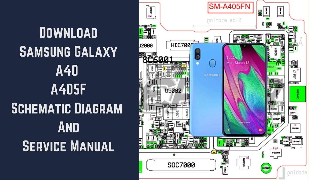
shema-samsung-a405f-rev03.zip
Size:
1.34 Mb
Format:
zip
Downloads:
32
File available for download
Download file
- Views: 43
- Category: Other files
See Also
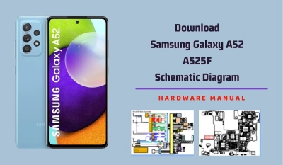
Схема Samsung Galaxy A52 A525F Schematic Diagram Cover Disassembly & Reassembly Electrical Part List Exploded View Product Specification Troubleshooting
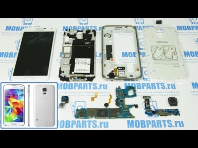

Схема RH-18/36/38 Schematic Diagrams Nokia Customer Care Solutions Schematics / Layouts 1AW_09 module RH-18/36/38 Issue 1 Table of Contents Page BB/RF connection block diagram v.0.0 Mjölner IC v.0.0 ed. 229 4 Power amplifier diagram v. 0.0 Baseband block diagram v. 0.0 Audio schematic diagram v. 1.3 Keyboard diagram v. 1.3 Flash memory diagram v. 2.0 Discrete capacitors for memory without VFlash1 v. 1.3 Discrete power v.1.3 Light filtering diagram, v.2. 0 RH* Old power discrete capacitors, v. 0.0 ed. Power resistor v. 0.0 ed RF/BB connection, v. 1.3 ed. SIM v. 1.3 ed. System connector v. 1.3 ed. UPP 8M diagram, v. 2.0 ed. 107 Discrete decoupling capacitors for UPP v,. 1.3 ed.10 Audio and Global Ground v. 0.0 RH* Component layout 1AW_07a, top side Component layout 1AW_07a, bottom side Test Points, Baseband